Precision optical filters and specialty optics
Precision filters and specialty optics are often closely tied to the way an instrument is designed, especially where spectral performance, geometry or substrate choice is tightly specified.
Helia develops wafer-level filters, micro-optics and specialised bulk optics for instrument and system builders working in defence, medical imaging, hyperspectral sensing, agri-tech, forensics and other demanding applications. That includes components with tightly defined spectral behaviour, difficult substrates or process flows that need to fit into a wider manufacturing sequence.
Who this is for
This page is for instrument and system builders who need filters or coated optics that are closely tied to the way their product works.
- OEMs developing medical, life-science and analytical instruments with tightly defined optical requirements.
- Suppliers of hyperspectral and multispectral imaging systems for defence, agriculture, remote sensing and industrial inspection.
- Designers of forensic and laboratory instruments, including mass spectrometry and specialised microscopy platforms.
- Detector, sensor and sub-system teams that need wafer-level filters, mosaic arrays or micro-optics integrated into a larger architecture.
- Manufacturers of specialist sensing and scientific instruments that require non-standard substrates, unusual wavelength bands or custom spectral behaviour.
If your system depends on a specific spectral shape, a detector mosaic, a micro-optic or a difficult substrate, this is the part of Helia built around those requirements.
The challenge
In many instruments, optical performance is concentrated in a small number of components: a filter edge that sets channel separation, a coated prism that shapes the signal path, or a detector array whose spectral regions are built directly into the wafer.
These parts are often closely tied to the architecture of the instrument, which means they are not easy to swap out without affecting calibration, sensitivity, spectral discrimination or mechanical integration.
The challenge increases when the requirement involves mosaic filters, micro-structured optics, tight edge behaviour, deep blocking, unusual wavelength bands or substrates such as CaF₂, ZnSe or silicon. At that point, standard catalogue parts and generic coating flows may not map cleanly onto the design.
Our solutions
Helia provides wafer-level filters, coated micro-optics and specialised bulk optics for customers whose instrument performance depends on tight spectral control, robust process sequencing and repeatable manufacture.
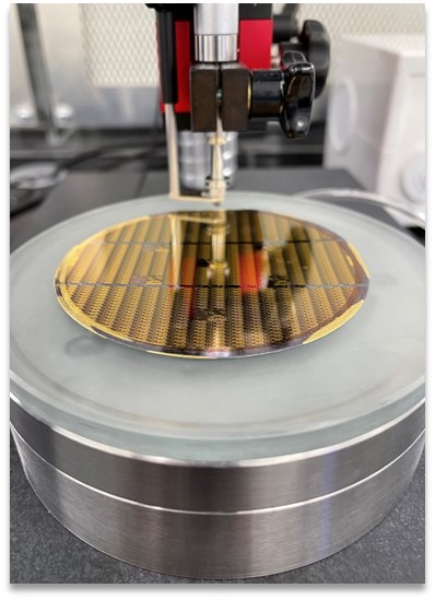
Wafer-level filters and detector mosaics
We process wafers that will become detector arrays by defining distinct regions through photolithography and depositing different filter stacks into those regions to create a mosaic of spectral responses across the array.
- Up to around fifteen separate deposition steps on a single wafer, each providing a different edge or bandpass function.
- Careful sequencing so that earlier coatings remain stable through later process steps and bake-outs.
- Thinning, dicing and final inspection carried out after the filter sequence is complete, reducing risk on fragile wafers.
This supports focal plane arrays and other detector architectures where each region of the wafer has to deliver a defined spectral window within the finished system.
Micro-optics and structured components
For wafers carrying microlenses, MEMS structures or other micro-optical features, we apply coatings to one or both sides and build the flow around the geometry and handling limits of the part.
- Designs that can combine mirror, beamsplitter, filter or AR functions across the component.
- Process flows developed to avoid damaging delicate surface relief or MEMS features.
- Measurement, dicing and inspection steps tailored to the scale and complexity of the structure.
The aim is not just to coat the part, but to make sure the coated micro-optic behaves consistently once assembled into the instrument.
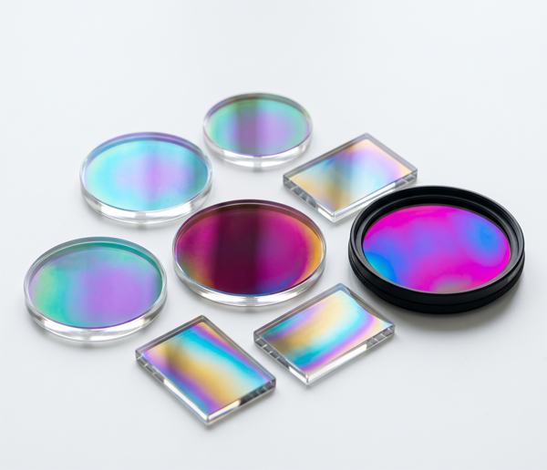
Bulk optics for demanding instruments
We also support a focused set of customers needing specialised coated bulk optics for analytical, cryogenic, defence and sensing applications where the optic is small in size but significant in system impact.
- Cleaning and coating flows adapted to substrates from glass and silicon through CaF₂, ZnSe and other challenging materials.
- Precision optical monitoring on selected systems for tight edge filters and more consistent spectral performance.
- Attention to the thermal, mechanical and environmental constraints of the finished instrument.
These parts are often deeply designed into the instrument, so stability, consistency and re-supply matter as much as the nominal spectrum.
Technical capabilities
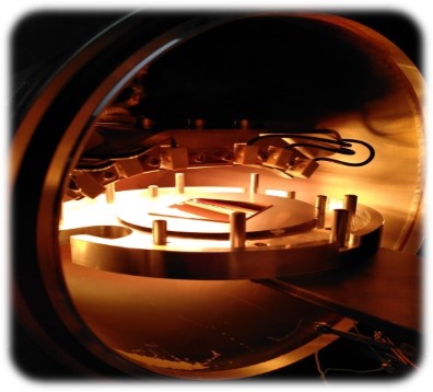
Helia’s coating plant combines ion-assisted electron-beam systems, magnetron sputter tools, thermal evaporation systems and IBS platforms, giving us a broad process base for filters and specialty optics.
Precision optical monitoring on selected tools improves control over steep edges and tightly defined spectral shapes, while our materials portfolio supports designs from the UV through the visible and into the long-wave infrared.
- Broad selection of oxides, fluorides, sulphides, selenides, tellurides, metals and mixed oxides.
- Process know-how across substrates including glass, silicon, CaF₂, ZnSe and other challenging materials.
- Design and modelling support to move from a target spectrum to a manufacturable stack.
- Metrology from 185 nm into the tens of microns to verify performance over the component’s working band.
This gives us the flexibility to handle unusual filter shapes, difficult substrates and application-specific optical requirements that do not sit comfortably within standard catalogue ranges.
How we work with you
Projects in this area often begin as technically demanding development work, then move into repeat production once the instrument architecture is fixed and market demand builds.
Define the component requirement
We start from the role the optic plays in the instrument: spectral targets, blocking, edge position, substrate, geometry, handling constraints and operating environment.
Design the stack and process flow
We translate the target optical behaviour into a manufacturable design, taking into account sequencing, photolithography, coating compatibility and downstream processing.
Prototype and measure
Initial parts are produced and characterised so we can compare measured performance against the required spectral and physical behaviour.
Refine for the real instrument
We iterate where needed to improve fit with the system, whether that means spectral adjustment, process robustness, handling changes or tighter control of variation.
Lock down repeatable manufacture
Once the design is frozen, we establish a stable production route with the documentation, inspection and process control needed for ongoing supply.
Talk to us about your filters and optics
If your system depends on a filter edge, a mosaic detector array or a non‑standard substrate, and the catalogue options are not quite right, we would be happy to explore whether we can help.
FOLLOW US
Contact Us
Helia Photonics Ltd
Rosebank Technology Park
Livingston
West Lothian
Scotland, UK
EH54 7EJ
+44 (0)1506 414800