Coatings and back‑end processing for quantum technology
Quantum systems often have new requirements of optics and this can fall outside the standard catalogue parts, so coatings and processes need to be engineered around the specific experiment or product.
From first‑stage cooling in lattice clocks to packaged sources for gravimetry and communications, quantum projects place tight, coupled demands on wavelength, power, linewidth and stability. Helia works with UK and international quantum programmes to design coatings, windows and handling processes so your chosen architecture can move from lab demonstrator towards commercial deployment.
Who this is for
We typically work with teams building quantum computers, quantum sensors and optical clocks, and with the OEMs who supply lasers, optics and instrumentation into that supply chain.
- Teams building neutral‑atom, ion‑trap, photonic or superconducting processors and trying to move beyond first‑run experiments into repeatable platforms.
- Companies developing quantum sensing and timing systems (atomic clocks, gravimeters, magnetometers).
- University and national‑lab groups with ambitious AMO or Rydberg programmes that need more than one‑off prototypes.
- OEMs building quantum‑ready lasers, optics and metrology tools.
If you recognise yourself in that list and your work depends on thin films, coated windows, chip facets or detector filters, we are set up to help.
The quantum optics challenge
Quantum systems run close to their limits. Small losses and drifts that are acceptable in classical optics can quietly degrade or break performance in quantum experiments and products.
Our customers repeatedly face a mix of challenges:
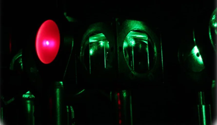
- Multiple critical wavelengths through the same surface. A single window or optic has to handle pump, probe, trap and cooling beams with low loss and minimal parasitic etalons.
- Ultra‑high vacuum and cryogenic environments. Coatings must get through UHV bake‑outs, repeated temperature cycling and long service without noticeable outgassing or drift.
- Tight loss budgets. Loss in cavities, waveguides and filters adds up across a system; reducing it where you can improves count rates, contrast or sensitivity and gives more margin elsewhere in the design.
- Rapidly evolving architectures. As teams uncover new constraints, they adjust their architectures, and the associated optics and coatings have to follow.
Standard catalogue optics and general‑purpose AR coatings are often enough to get early experiments running, but custom coatings and windows are typically needed to reach stable, repeatable quantum systems.
How Helia helps quantum teams
Helia’s quantum work grew out of demanding semiconductor, telecoms and defence programmes, and then into optical clock and superconducting projects. That background means we approach quantum optics with the same process control and repeatability we use in semiconductor manufacturing.
Application‑specific windows and filters
We collaborate with quantum clock and cold‑atom teams to design species‑specific sets: vacuum windows and optics optimised for the pump, probe, trap and cool wavelengths for a given atom or transition.
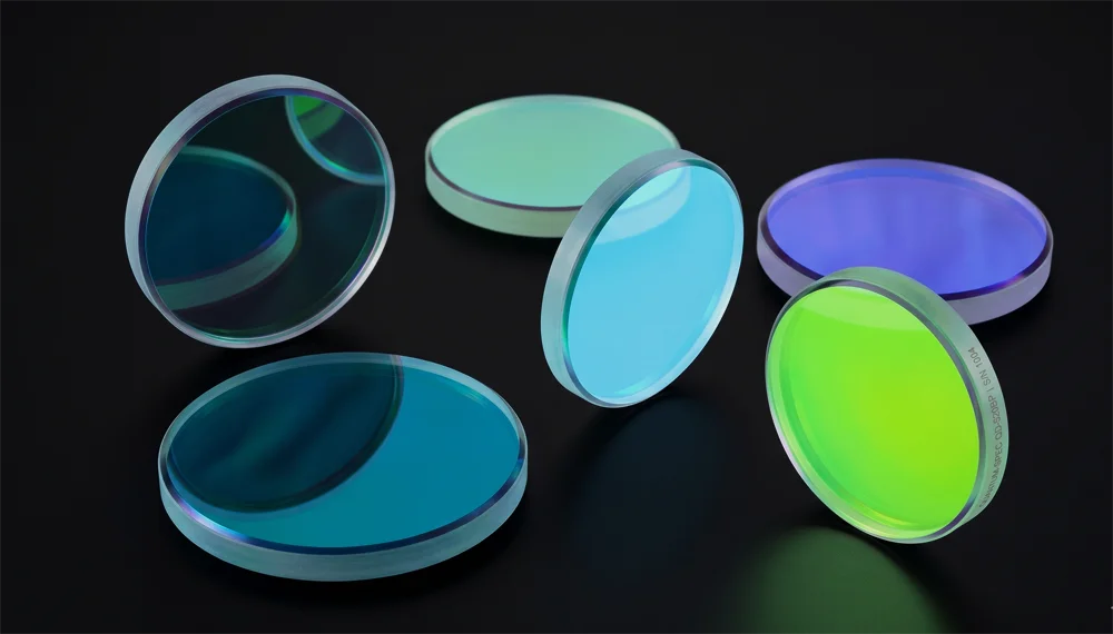
- Broadband or multi‑wavelength AR coatings tuned to your actual laser set.
- Substrates and processes chosen for UHV and bake‑out compatibility.
For quantum setups where weak signals sit next to strong pump beams, we design narrowband and edge filters to separate the two while maintaining high transmission and stability.
Coatings and back‑end for photonic quantum chips
Integrated photonics makes the chip facets and on‑chip thin‑film stacks as important as the waveguides themselves. Helia routinely takes part‑processed III–V and hybrid wafers and returns usable photonic devices, including:
- Thinning, back‑metal and cleave/stack processes on III–V and hybrid wafers.
- AR coatings on chip facets to manage back‑reflection and loss.
- HR and filter stacks on facets or local regions for cavities and on‑chip filtering.
We support InP and other III–V photonics foundry customers as a back‑end partner, across applications from quantum devices to data‑comms and AI hardware. The same infrastructure supports quantum‑specific PICs and laser chips.
Superconducting and advanced thin films
For superconducting‑based quantum circuits, we work with ultra‑thin superconducting films such as niobium, FeSeTe and tantalum nitride as part of custom thin‑film stacks. Combined with our ability to design and build dedicated deposition hardware, this gives you a way to:
- Explore new material combinations and thicknesses without having to build your own coating line.
- Turn promising R&D stacks into repeatable, documented processes once your design stabilises.
Capabilities you can build on
Helia is a small, technically deep team with over two decades of experience in high‑end photonics.
- Broad materials and spectral range. More than 125 coating materials, covering roughly 0.4–30 μm, including oxides, fluorides, sulphides, selenides, tellurides, metals, semiconductors and transparent conductive oxides.
- Multiple deposition platforms. Ion‑assisted e‑beam, magnetron sputtering, thermal evaporation and ion‑beam sputtering, all tied into in‑house control software for precise, repeatable thickness control..
- Strong metrology and test. Variable‑angle spectrophotometry, FTIR into the mid‑IR, Raman microscopy, SEM and proprietary electro‑optic test platforms (HelTest, HelOptr) so you can see how coatings and devices actually perform, not just what the model predicted.
- Automation where it matters. Robotics for bar and wafer handling (Helbot) and automated inspection with machine‑learning‑based grading (Helview, HelAI) support stable, high‑volume processing once a coating or BEoL flow is locked down.
Because we design and build much of our own hardware and software, we can adjust processes to unusual requirements instead of forcing your design to fit a fixed toolset.
Working with Helia on quantum projects
Most quantum engagements start with a conversation about a specific problem:
- A vacuum window or cell that needs to handle several precise wavelengths with minimal loss.
- A chip facet that is reflection‑sensitive at a particular quantum‑relevant wavelength.
- A set of filters or cavity mirrors whose performance is currently constraining the system.
- A superconducting or exotic thin‑film stack that needs to be explored without building new tools from scratch.
From there we typically:
- Clarify the optical and environmental requirements, including any constraints from existing designs or vendors.
- Propose one or more coating or process options, including any trade‑offs.
- Produce a small batch for evaluation, with the metrology data you need for your own system‑level modelling.
- Support further iterations or move into steady, repeatable supply when your design is fixed.
Quantum roadmaps keep moving as the physics and the engineering mature, and we’re set up to adapt our work with you over time.
Talk to us
If you are planning or already building a quantum system and you know coatings, windows or chip facets are on the critical path, we would be happy to explore whether we can help.
FOLLOW US
Contact Us
Helia Photonics Ltd
Rosebank Technology Park
Livingston
West Lothian
Scotland, UK
EH54 7EJ
+44 (0)1506 414800