
CORE MARKET: Quantum technology
Quantum coatings and processing
Quantum systems often need optics beyond standard catalogue specifications. Helia engineers coatings, windows and back-end processes around your wavelengths, operating environment and route to production.
0.4–30 µm
SPECTRAL COVERAGE
125+
COATING MATERIALS
UHV
COMPATIBLE PROCESSES
R&D to supply
PROJECT PATHWAY
who this is for
For teams turning quantum physics into repeatable hardware
Helia works with quantum system developers and the OEMs supplying lasers, optics and instrumentation into the same value chain.
01
Quantum computing teams
Neutral-atom, ion-trap, photonic and superconducting platforms moving beyond first-run experiments.
02
Sensing and timing developers
Teams building atomic clocks, gravimeters, magnetometers and other fieldable quantum instruments.
03
Research programmes
University and national-laboratory groups with ambitious AMO or Rydberg programmes that need more than one-off prototypes.
04
Quantum supply-chain OEMs
Manufacturers developing quantum-ready lasers, optics, coated windows and metrology tools.
The quantum optics challenge
Small optical compromises become system-level constraints
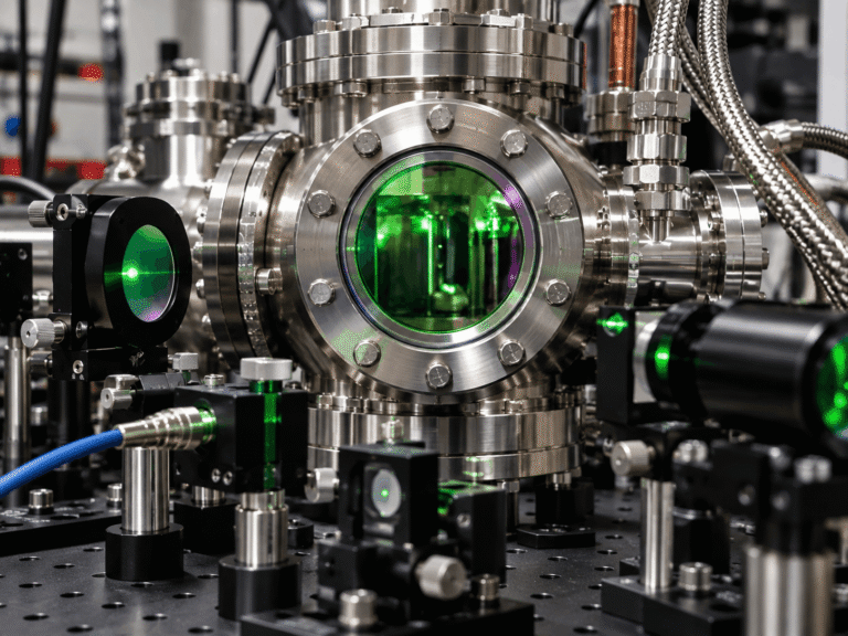
Quantum systems operate close to their limits. Losses and drifts that may be acceptable in classical optics can quietly reduce count rates, contrast, coherence or sensitivity.
Several critical wavelengths, one surface
A window may need to carry pump, probe, trap and cooling beams with low loss and minimal parasitic etalons.
UHV, bake-out and cryogenic operation
Coatings must tolerate demanding environments, thermal cycles and long service.
Tightly controlled loss budgets
Loss across cavities, waveguides and filters accumulates across the architecture.
How helia helps
Optical and thin-film engineering around the application
Helia brings semiconductor-grade process control to quantum projects, supporting exploratory work and a practical route into repeatable manufacture.
01 / Optical interfaces
Application-specific windows and filters
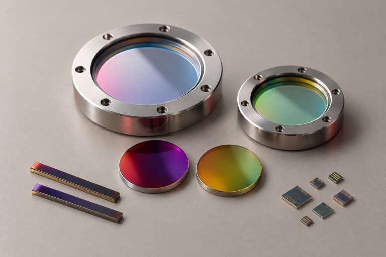
Species-specific sets for quantum clocks and cold-atom systems, optimised around the pump, probe, trap and cooling wavelengths.
- Broadband or multi-wavelength AR coatings
- UHV and bake-out-compatible processes
- Narrowband and edge filters
02 / Integrated photonics
Coatings and back-end for quantum chips
Processing for part-complete III-V and hybrid wafers.
- Thinning, back metal, cleave and stack
- AR coatings on chip facets
- HR and filter stacks
03 / Advanced materials
Superconducting and advanced thin films
Custom ultra-thin-film stacks using materials such as niobium, FeSeTe and tantalum nitride.
- Explore new material combinations
- Develop documented processes
The Helia difference
Capabilities you can build on
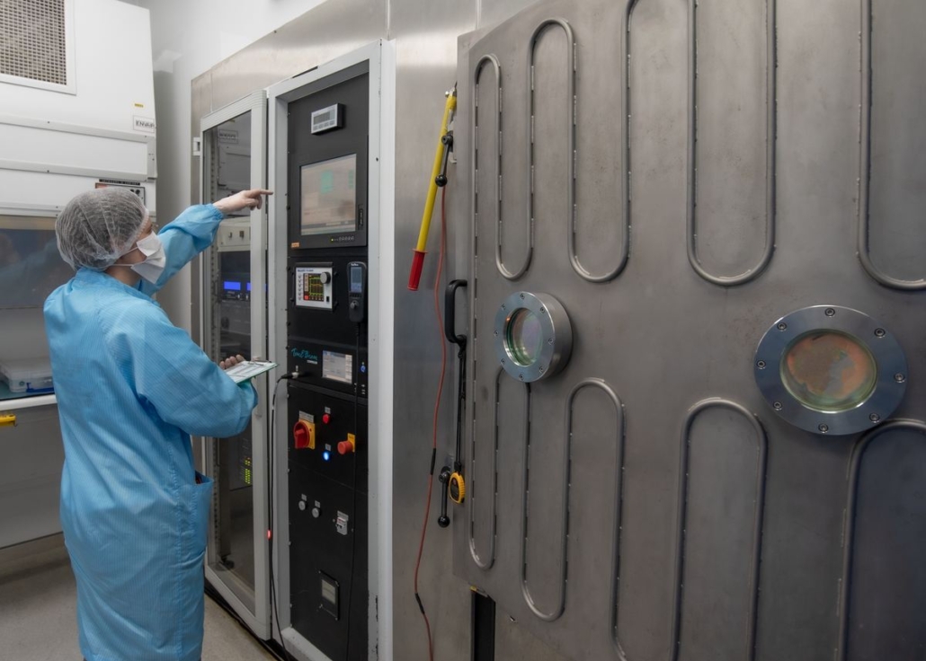
A technically deep team, multiple deposition routes and in-house metrology allow the process to adapt to the device rather than forcing the device into a fixed toolset.
01
Broad materials portfolio
More than 125 materials, covering oxides, fluorides, chalcogenides, metals, semiconductors and transparent conductive oxides.
02
Multiple deposition platforms
Ion-assisted e-beam, magnetron sputtering, thermal evaporation and ion-beam sputtering.
03
Metrology and test
Variable-angle spectrophotometry, FTIR, Raman microscopy, SEM and proprietary electro-optic test platforms.
04
Automation where it matters
Automated handling and machine-learning-supported inspection help maintain repeatable processing at scale.
Working with Helia
From optical problem to repeatable supply
Most engagements start with one clearly defined constraint: a multi-wavelength window, reflection-sensitive facet, limiting filter or new thin-film stack.
Define the operating requirements
Clarify optical, environmental and integration constraints.
Evaluate process options
Develop practical routes and make performance and manufacturing trade-offs visible.
Produce and measure an evaluation batch
Supply a small batch with the metrology needed for system-level evaluation.
Iterate or move into steady supply
Refine the design, then lock down a documented and repeatable production process.
Are coatings, windows or chip facets on your critical path?
Tell us what the system needs to do, where current optics are limiting it and how far the design has progressed.
Location
Livingston, Scotland.
FOLLOW US

Contact Us
Helia Photonics Ltd
Rosebank Technology Park
Livingston
West Lothian
Scotland, UK
EH54 7EJ
+44 (0)1506 414800