
CORE SERVICE: FACET COATINGS
Facet coatings for sensitive photonic devices
Precision facet coatings, engineered with device makers to deliver performance, reliability and yield at every stage of production.
What are facet coatings?
Ultra-thin coatings that control how light behaves at the facet
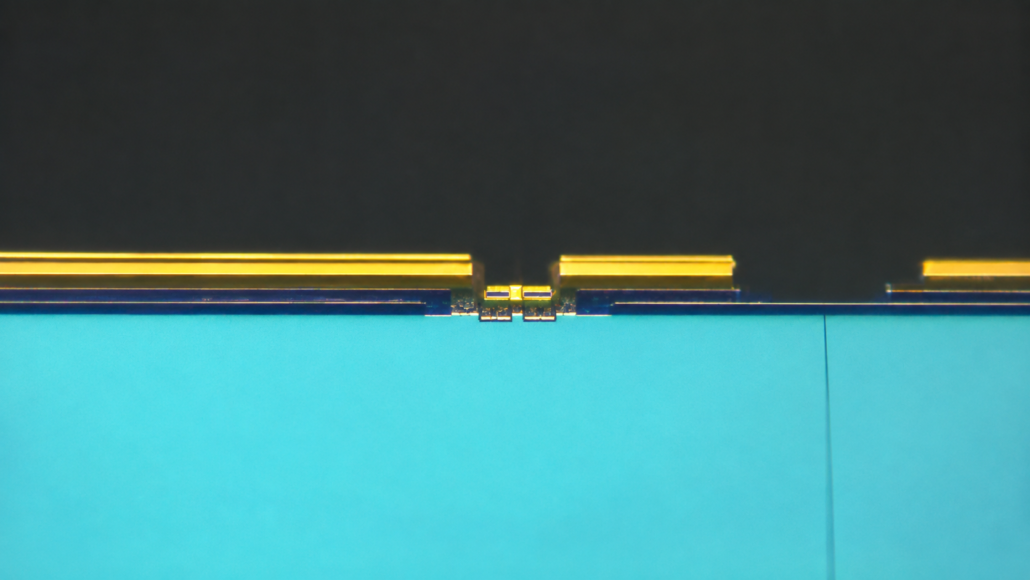
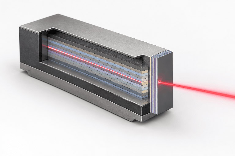
Facet coatings are functional ultra-thin coatings applied to the end face (facet) of photonics devices such as laser diodes, photonic integrated circuits and semiconductor devices. By precisely controlling how light behaves at the facet, they radically enhance a device’s efficiency, stability and longevity.
The leading reliability risk for high-power laser diodes is catastrophic optical mirror damage (COMD), where facet-surface defects trigger localised heating and thermal runaway. Correct facet coating, combined with proper etch and passivation of the surface beforehand, pushes the COMD threshold higher and extends operating lifetime
The facet challenge
Where performance is won or lost
When it comes to photonic and semiconductor devices, the facet is often where performance is won or lost. A facet must precisely control light while withstanding mechanical handling, thermal stress, and long-term operation. To achieve this, we develop custom solutions specific to your device, its packaging and its application.
Optimised behaviour without added instability
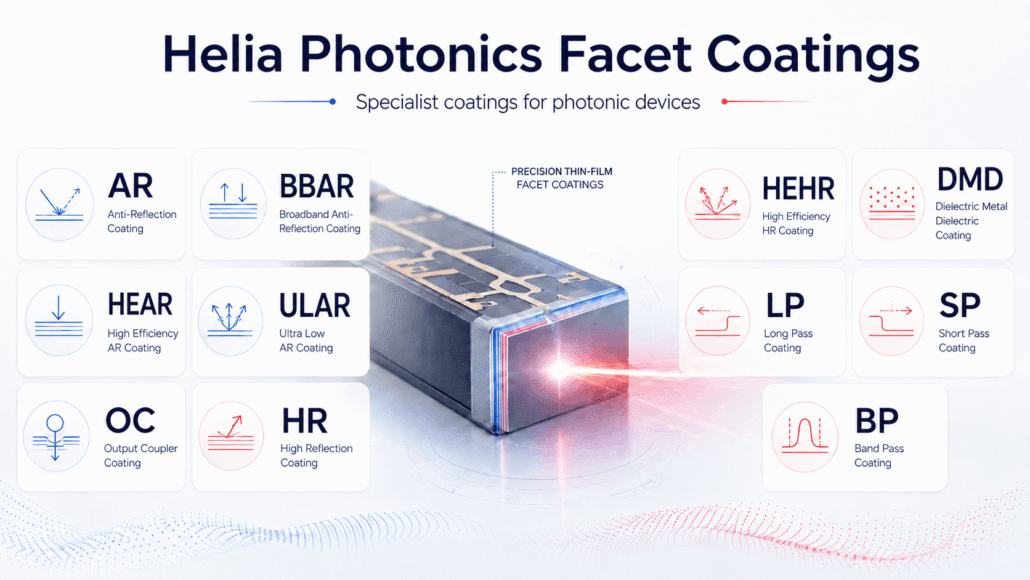
We engineer custom coatings providing anti-reflection, high-reflection or partial reflection without introducing excess absorption, thermal stress or instability over time.
Specialist surface preparation and assessment
Cleaved edges, etched facets and compound structures can introduce damage, contamination and native oxides. Our etch and passivation processes address these surface states before coatings are applied, ensuring your substrate is impeccably prepared and directly improving COMD resistance.
Expert consideration of operating conditions
Our specialty coatings counter the effects of high optical powers, pulsed formats, temperature cycling, hermetic packaging requirements and environmental exposures which can erode poorly designed coatings.
Fabrication processes which are optimised for repeatability
We ensure consistent handling, fixturing and process control throughout fabrication to support high repeatability and yields.
Why work with Helia?
Solutions built around your device, not a standard catalogue
Every photonic device has unique optical and mechanical challenges. Rather than forcing your design into a standard coating process, we develop facet coating solutions around your device, your application and your performance goals.
Coating strategies matched to your device
We customise our designs around your device architecture and application, rather than constraining our customers to a small catalogue of designs.
- Coatings for emitters, bars and arrays where back-reflection inhibits device performance.
- Critical facet coatings for PICs and hybrid devices.
- Customisation for your operational parameters and environmental conditions.
Surface-aware processes and handling
Our facet solutions are built around the reality of fragile edges, contamination risks, and tight geometries.
- Process flows that account for cleaving, cleaning and surface conditioning before coating.
- Fixturing and handling developed around your specific bar, chip or wafer geometry.
- Detailed consideration of how surfaces are protected, stored and transported between process steps.
Comprehensive coating capabilities
Our 25 years of experience in thin film coatings empowers us to combine the right materials, and deposition techniques to meet your requirements.
- Multiple deposition platforms.
- Broad portfolio of materials including oxides, fluorides and dielectrics.
- Process expertise across III-V material systems including GaAs, InP, GaSb and GaN, each with distinct surface chemistry and passivation requirements.
- Coatings for complex surfaces, such as fibre optic connectors.
Routes from development to production
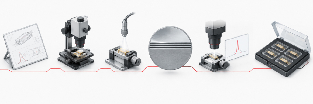
Whether you’re proving a new concept or scaling into production, we provide a complete path from prototyping to repeatable manufacturing.
- Feasibility batches to test concepts and identify constraints.
- Iterative process development to ensure high yield and repeatability.
- Translation into a repeatable and well-documented process.
Metrology and inspection
Our facilities contain a wealth of metrology and inspection equipment to ensure full characterisation of your product.
- Proprietary visual inspection equipment to ensure
- Comprehensive optical analysis through Raman and Fourier-transformed spectroscopy.
Automation where it matters
Our in-house developed handling and inspection equipment ensures high yields.
- Our proprietary handling equipment, HELBOT™ ensures individual chips and bars are handled with consistent pressure to maximise yield.
- Our proprietary visual inspection equipment, HELVIEW™ supports accurate and time-efficient inspection.
How we work with you
A clean route from development to repeat supply
Facet projects usually start with a specific difficulty, a device that is reflection-sensitive, a reliability concern, or a yield problem, and then evolve as the architecture matures. Helia’s process is designed to surface constraints early and support a clean route from development to repeat supply. Throughout, the emphasis is on clear communication about what is known, what is still being explored and how changes at the facet interact with the rest of the device.
Every successful solution starts with the right conversation
Whether you are developing a new product, scaling into production, or looking to improve yields, our engineers can help you identify the right coating strategy for your application.
Website
www.helia-photonics.com
Location
Livingston, Scotland.
FOLLOW US

Contact Us
Helia Photonics Ltd
Rosebank Technology Park
Livingston
West Lothian
Scotland, UK
EH54 7EJ
+44 (0)1506 414800